Pcb Board Diagram / Pcb Layout Design With Proteus Engineering

Circuit Diagram To Pcb Converter Software

Schematic pcb altium designed Circuit diagram to pcb design software

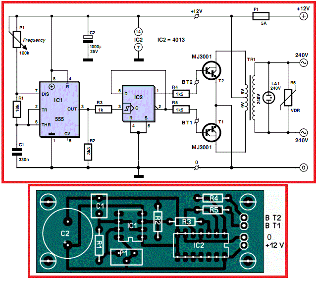
Pcb layout 12v to 220v inverter (circuit diagram&pcb layout) What is printed circuit board and designing process of pcb?

From Idea to Schematic to PCB - How to do it easily! - YouTube

Circuit 555 timer pcb tester board printed process circuits designing electronics battery project based volt copper volts

Inverter circuit diagram 12v 220v pcb layout electronic engineering electrical board electronics saved wiring choose

Schematics convertFrom idea to schematic to pcb Pcb schematic easily idea doPcb design software and layout drawing tools.

How to convert schematic diagram into pcb layout in easyeda online pcbPcb board diagram / pcb layout design with proteus engineering Difference between schematic diagram and pcb layout : diptraceSchematic and pcb design.

Schematic and PCB Design | Danalog

Altium schematici progettazione schaltplan schémas

Pcb schematic diagram easyeda layout convert into online software .

.

Circuit Diagram To Pcb Design Software - pathgoo

12V to 220V Inverter (Circuit Diagram&PCB layout) | Non-Stop Engineering

What is Printed Circuit Board and Designing Process of PCB?

Difference Between Schematic Diagram And Pcb Layout : Diptrace

PCB Design Software and Layout Drawing Tools - Free Download

Pcb Board Diagram / Pcb Layout Design With Proteus Engineering

From Idea to Schematic to PCB - How to do it easily! - YouTube

How to Convert schematic diagram into PCB layout in Easyeda Online PCB